Gas Purity Enhances Chips for Wireless Revolution
Most users of iPhones, iPads, and other wireless technology hardly imagine that gases are critical to the manufacture of the tiny chips that operate their devices. But, ultra-pure hydrogen chloride (HCl), hydrogen (H2), and nitrogen (N2) all play vital roles in the manufacture of super-fast, low-temperature, lower power consuming telecommunications chips.
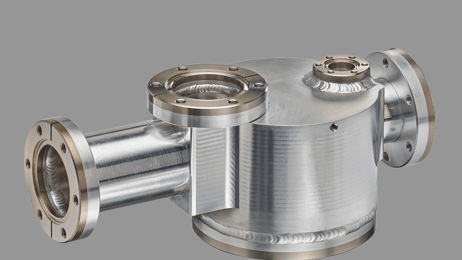
Underscore “pure” because the process of manufacturing tiny chips itself — a derivative of traditional epitaxy — actually invites contamination in an unexpected fashion. Epitaxial (epi) processing is used in specific types of semiconductor production, including advanced CMOS applications for microprocessors and other types of digital communications. This type of chemical vapor deposition (CVD) offers great benefits for wafers using silicon (Si) and germanium (Ge) materials that are critical building blocks for wireless technology. A predictable strain in the germanium lattice enhances the quality of the layers on a chip and therefore, the performance of the end-product. Facilitating a predicable strain dictates low thermal budgets in order to maintain doping profiles and prevent diffusion; hence, the emergence of so-called “Low Temperature Epitaxy.” But, as the search for yield enhancement and cost-effectiveness in advanced epitaxial processing progresses, unintended consequences can and do occur. For example, at high temperatures, moisture (H2O) and oxygen (O2) bake-off and interfacial oxidation defects are unusual. But, with the shift to lower temperature epitaxial processes (below 800°C), process engineers learned that O2 molecules still baked-off, but H2O molecules remained. Depending on the partial pressure of the gas, this residual H2O can deposit oxygen on the highly reactive wafer surface, leading to oxidation at the epi-substrate layer and in the epi layer.
But, as the search for yield enhancement and cost-effectiveness in advanced epitaxial processing progresses, unintended consequences can and do occur.”
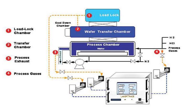
That makes moisture molecules a prime source of oxidation defects. Moisture can be introduced into the process chamber from a variety of sources, including aging purifiers; wafer handling chambers (WHC) upon introduction of the wafer; the carrier and dopant gases; insufficient purging or baking; and leaks in the tool itself. The research consortium for international semiconductor manufacturing (IMEC) has studied moisture effects in low-temperature epi since 2005. Dr. Roger Loo, Senior Scientist Si, SiGe, and Ge epitaxy at IMEC in Leuven, Belgium, notes, “Normally, the wafer susceptor is coated with a protective Si layer just before loading. If the dichlorosilane (DCS) is of bad quality, this protective layer acts as a contamination source during further processing.”
... to continue reading you must be subscribed