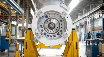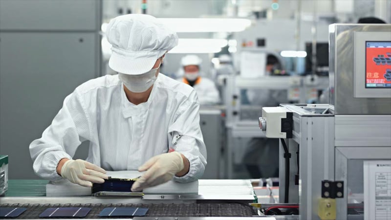
New Challenges in Photovoltaic Manufacturing
Manufacturers of photovoltaic (PV) devices are under constant pressure to improve the cost per watt in order to drive market growth and compete with other forms of energy. Reducing manufacturing costs has enabled significant market growth, but continuing with this approach alone will meet with diminishing returns and profitability for manufacturers.
Increasing the number of watts from the same device will also reduce the cost per watt, so there is a lot of recent attention on increasing efficiency. New materials and new applications are required to achieve these gains and this article describes some of the approaches being taken.
Backside Passivation
The photovoltaic effect relies on light generating free electrons from the photovoltaic material. Any loss of these electrons on their path to the electrical contacts reduces the efficiency of the device. Surface recombination, where electrons can combine with dangling bonds at the silicon surface, is one such mechanism and becomes more important to reduce as devices get thinner. Passivation of the surfaces ties up all the dangling bonds and provides a more neutral electrical surface to minimize electrical recombination. One material being studied as a passivation layer is aluminum oxide deposited by chemical vapor deposition (CVD) using tri-methyl aluminum (TMA). Results show that this process can lead to a one percent improvement in cell efficiency. TMA is routinely used for LED manufacture, and so the handling challenges are known but will be new to PV manufacturers.
N-Type Wafers
Traditionally p-type wafers as used by the semiconductor industry have been the substrate used for crystalline silicon (Si) solar cells. With the solar wafer market becoming important in its own right, manufacturers are now looking at what sort of wafers would be best for PV devices. P-type wafers are bulk doped with boron, but boron forms defects with oxygen present in the bulk material when exposed to light (a process known as light induced degradation) causing the efficiency of the cell to drop over time. Boron doped devices are also more sensitive to metal impurities, which can also cause recombination. N-type wafers, which are bulk doped with phosphorus, do not exhibit the same light induced degradation and, due to the difference in carrier type (holes rather than electrons), there is much less recombination due to metal impurities. The use of ntype wafers can lead to an increase in cell efficiency of up to one percent.
... to continue reading you must be subscribed