Loading...
Loading...
applied-materials-to-build-4bn-semiconductor-research-centre-in-silicon-valley

Applied Materials to build $4bn semiconductor research centre in Silicon Valley

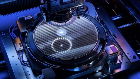
US manufacturing firm Applied Materials has unveiled plans to build what it says will be the world’s largest and most advanced facility for collaborative semiconductor process technology and manufacturing equipment research and development (R&D).

Described as a “landmark investment”, the multi-billion-dollar Equipment and Process Innovation and Commercialisation (EPIC) Centre will be located at an applied campus in Silicon Valley, California and feature a cleanroom for collaborative innovation with chipmakers, universities, and ecosystem partners.

To create the EPIC Centre, Applied Materials expects to make gross, incremental capital investments of up to $4bn over the next seven years. The innovation centre is expected to be completed by early 2026 and become the nexus of more than $25bn in company R&D investments in the first 10 years of operations.

It is hoped the EPIC Centre will accelerate development and commercialisation of foundational technologies required by the global semiconductor and computing industries.

With that, Applied Materials hopes to reduce the time it takes industry to bring technologies from concept to commercialisation by several years, while increasing commercial success rates of new innovations.

Gary Dickerson, President and CEO of Applied Materials, notes the semiconductors are now more critical to the global economy than ever before and the technology challenges that the industry faces are becoming more complex.

“This investment presents a golden opportunity to re-engineer the way the global industry collaborates to deliver the foundational semiconductor process and manufacturing technologies needed to sustain rapid improvements in energy-efficient, high-performance computing,” he added.

The scale of Applied Materials’ investment is contingent upon receiving support from the US government through provisions of the CHIPS and Science Act.

Signed into law by President Joe Biden in August 2022, the ‘historic’ $52bn CHIPS Act looks to place the US as a leader in the semiconductor market and to revitalise domestic manufacturing and make the US competitor with the likes of China and Korea.

The CHIPS Act sets aside funding for new semiconductor programmes, including $39bn for a grant programme available to semiconductor manufacturers as well as equipment and materials suppliers.

The Act also includes $2bn for the legacy chips used in automobiles and defence systems, $13.2bn in R&D and workforce development and $500m to provide for international information communications technology security and semiconductor supply chain activities


About the author
Related Posts
No comments yet
Get involved
You are posting as , please view our terms and conditions before submitting your comment.
Loading...
Loading feed...
Please wait...